
What Is CAE Simulation?
Computer-aided engineering, commonly known as CAE, uses simulation software to analyze product performance before physical manufacturing. In electronics development, CAE helps engineers understand how a PCB or electronic system may behave under electrical, thermal, mechanical, and environmental conditions.
Instead of relying only on repeated physical prototypes, engineering teams can use simulation to identify design risks earlier. This helps reduce development cost, shorten project timelines, and improve product reliability before the board enters production.
Why CAE Matters for PCB Design
Modern PCBs are becoming smaller, denser, and more powerful. Components are placed closer together, signal speeds are higher, and thermal loads are more difficult to manage. A design that looks correct in the layout tool may still face problems in real-world use.
CAE simulation helps engineers answer practical questions before fabrication. Will a power component overheat? Is the board stack-up suitable for high-speed signals? Can the enclosure provide enough airflow? Will vibration or mechanical stress affect solder joints or connectors? These questions are easier and less expensive to address before production begins.
Common CAE Applications in Electronics
Thermal simulation is one of the most common CAE applications for PCB design. It helps engineers locate hot spots, evaluate heat spreading through copper layers, compare component placement options, and test the effect of airflow, heat sinks, or thermal vias.

Signal integrity simulation is used for high-speed digital designs. It helps verify controlled impedance, reflections, crosstalk, timing margins, and routing quality. For products using fast interfaces, signal integrity analysis can prevent communication errors and unstable performance.
Mechanical simulation can evaluate board bending, vibration, drop impact, and connector stress. This is especially important for automotive electronics, industrial devices, portable products, and any system exposed to movement or harsh operating conditions.
Electromagnetic simulation can help identify electromagnetic interference risks. Poor grounding, return path issues, high-current loops, and fast-switching signals may create EMI problems that are difficult to solve after manufacturing. CAE gives engineers a way to study these risks earlier.
Typical CAE Workflow for PCB Projects
A CAE workflow usually begins with design data. Engineers may import PCB layout files, mechanical enclosure models, component properties, material information, and operating conditions. The simulation model is then prepared by defining geometry, materials, power losses, boundary conditions, and analysis goals.
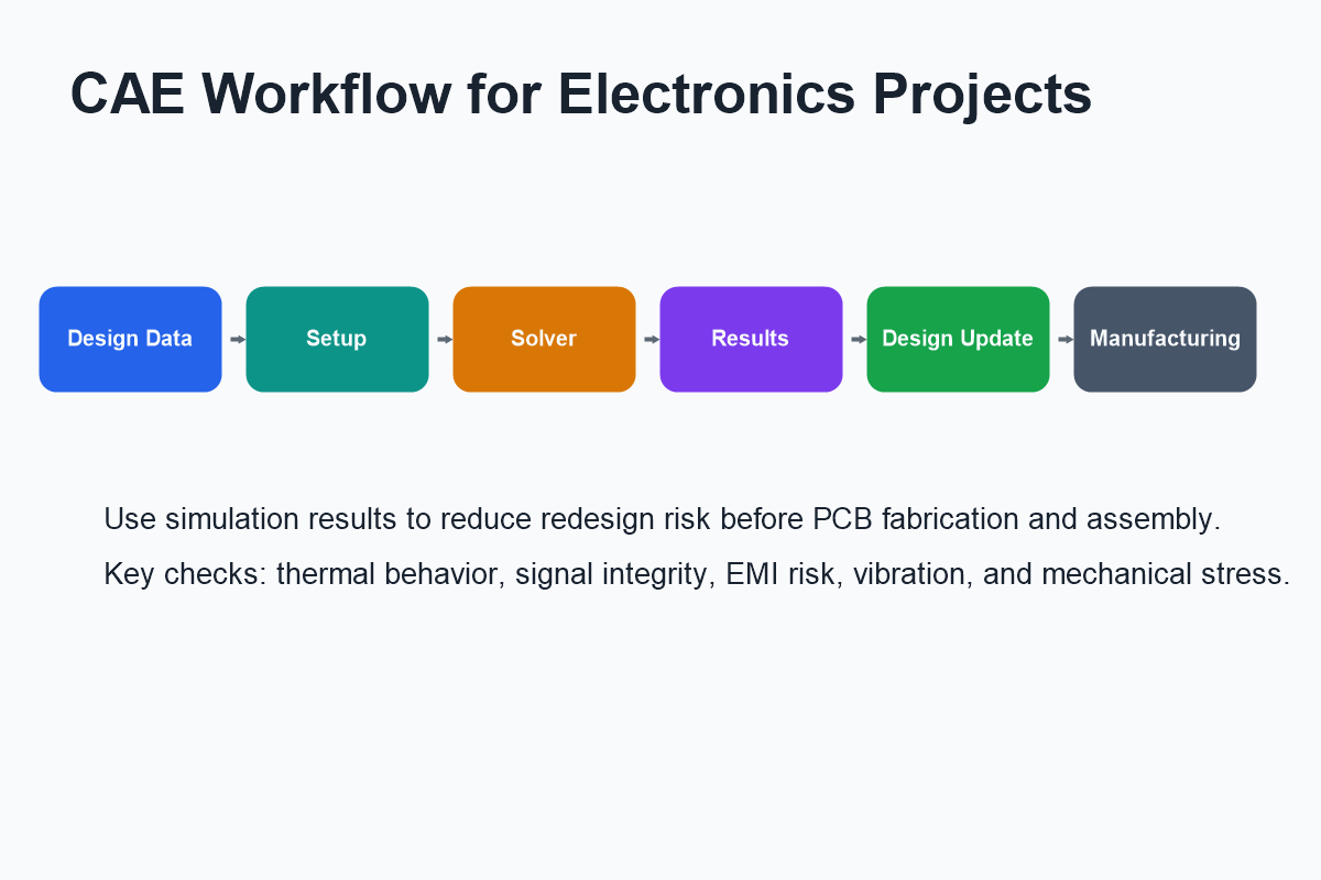
After setup, the solver calculates results based on the selected physics. Depending on the project, this may include temperature distribution, airflow, deformation, stress, voltage behavior, signal performance, or electromagnetic fields.
The final step is reviewing the results and improving the design. Engineers may adjust component placement, add thermal vias, change copper areas, improve grounding, update the stack-up, modify enclosure vents, or revise routing. The goal is not only to pass simulation, but to make better engineering decisions before the PCB is manufactured.
How Simulation Reduces Prototype Risk
Physical prototypes are still important, but they are expensive and time-consuming when used as the only validation method. If a serious issue is discovered after fabrication, the team may need to redesign the board, order a new prototype, and repeat assembly and testing.
CAE simulation reduces this risk by finding many problems before the first prototype is built. It also allows engineers to compare multiple design options quickly. For example, a team can test different heat sink sizes, copper pours, airflow paths, or component locations without waiting for new boards.
CAE and PCB Manufacturing
Simulation is most effective when it is combined with practical manufacturing knowledge. A design may perform well in simulation but still need to follow PCB fabrication and assembly rules. Trace width, spacing, via size, layer count, material selection, solder mask clearance, and panelization all affect whether the design can be produced reliably.
For this reason, CAE should work together with design for manufacturability review. When simulation results, layout rules, and manufacturing feedback are considered together, engineering teams can reduce redesigns and move from prototype to production more smoothly.
Conclusion
CAE simulation gives PCB designers and electronics engineers a better way to predict product behavior before manufacturing. It helps identify thermal, signal, mechanical, and electromagnetic risks early in the design cycle.
For modern electronics, simulation is not just an advanced engineering option. It is an important tool for improving reliability, reducing development time, and building products that are ready for real-world operating conditions.