
What Is an HDI PCB?
HDI PCB stands for high-density interconnect printed circuit board. It refers to a PCB technology that uses finer lines, smaller vias, higher wiring density, and more advanced layer structures than conventional circuit boards. HDI technology allows engineers to place more components and interconnections in a smaller area, which is especially important for compact and high-performance electronic products.
HDI PCBs are commonly used in smartphones, wearable devices, communication modules, medical electronics, aerospace systems, automotive electronics, high-speed computing products, and other applications where space, performance, and reliability are all important.
Why HDI PCB Technology Is Important
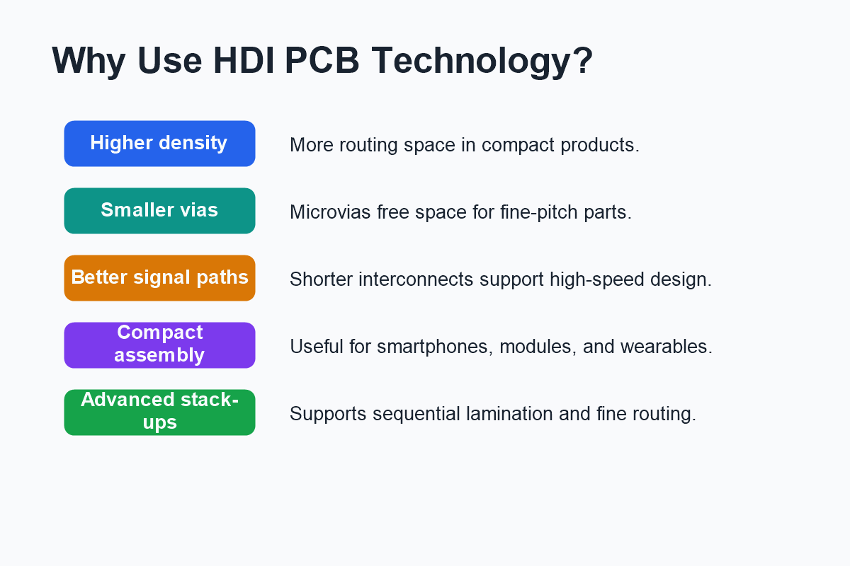
Modern electronic products are becoming smaller, thinner, and more powerful. At the same time, many designs require faster signal transmission, higher component density, and more complex power distribution. Traditional PCB structures may not provide enough routing space for fine-pitch components, dense BGAs, or high-speed interfaces.
HDI PCB technology helps solve these challenges by using microvias, thin dielectric layers, fine traces, and sequential lamination. These features give designers more routing flexibility and make it possible to create compact boards without sacrificing performance.
Key Features of HDI PCBs
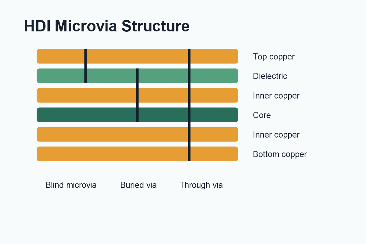
The most recognizable feature of HDI PCBs is the use of microvias. A microvia is a very small via, usually created by laser drilling, that connects one layer to an adjacent layer or to a nearby internal layer. Compared with mechanically drilled vias, microvias take up less space and allow traces to pass through dense component areas more easily.
HDI PCBs may also use blind vias, buried vias, via-in-pad structures, and fine-line routing. These design options help reduce board size and improve routing efficiency. In many cases, HDI technology allows a product to use fewer board layers than a conventional design with the same circuit complexity.
Common HDI Stack-Up Types
HDI stack-ups are often described by build-up structures such as 1+N+1, 2+N+2, or more advanced sequential lamination designs. In a 1+N+1 structure, one build-up layer is added on each side of a conventional core. In a 2+N+2 structure, two build-up layers are added on each side, allowing more complex microvia routing.
The right stack-up depends on routing density, component pitch, signal requirements, board thickness, cost target, and manufacturing capability. Choosing the stack-up early is important because it affects material selection, via design, impedance control, and production yield.
HDI PCB Manufacturing Workflow
HDI PCB manufacturing is more demanding than standard PCB fabrication. The process may include laser drilling, copper plating, sequential lamination, fine-line imaging, controlled etching, via filling, surface finishing, and electrical testing. Each step must be tightly controlled to maintain reliability and yield.
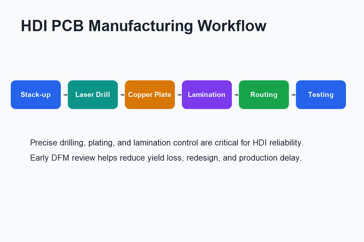
Laser drilling is especially important because microvia quality directly affects electrical and mechanical performance. Poor drilling, weak plating, voids, or misalignment can lead to reliability problems. For this reason, HDI projects require close coordination between the designer and the PCB manufacturer.
Design Considerations for HDI PCBs
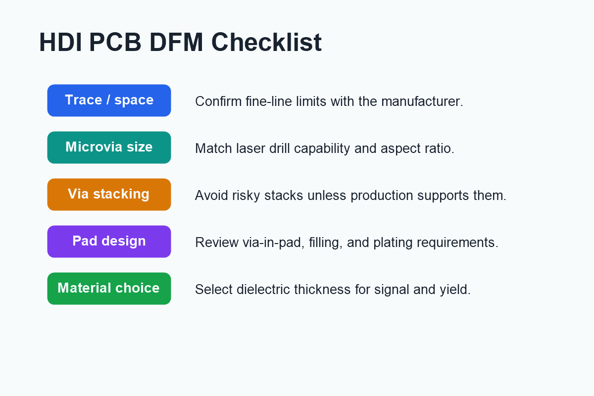
HDI PCB design should begin with manufacturability in mind. Designers need to confirm minimum trace width and spacing, microvia diameter, pad size, via-in-pad requirements, dielectric thickness, copper thickness, aspect ratio, and layer count with the manufacturing partner.
Via design is one of the most critical areas. Stacked microvias may be useful for very dense routing, but they can increase manufacturing risk if the process is not well controlled. Staggered microvias are often more reliable and may be easier to manufacture. The best choice depends on the board structure, reliability requirements, and supplier capability.
Signal integrity is another important consideration. Fine traces, high-speed interfaces, and dense routing can create challenges with impedance control, crosstalk, return paths, and power integrity. A good HDI layout should use proper reference planes, short signal paths, clean ground structures, and careful stack-up planning.
Benefits of HDI PCB Design
HDI PCBs provide several practical benefits. They make it possible to reduce board size, support fine-pitch components, improve routing density, and shorten interconnect paths. Shorter paths can improve signal performance and reduce parasitic effects in high-speed designs.
HDI technology can also improve product integration. By placing more functions on a smaller board, engineers can create lighter, thinner, and more compact products. This is valuable in portable electronics, smart devices, wireless modules, and advanced embedded systems.
Challenges and Cost Factors
Although HDI technology offers many advantages, it also adds manufacturing complexity. Laser drilling, sequential lamination, via filling, fine-line control, and advanced inspection can increase cost compared with standard PCB fabrication. Yield is also more sensitive to design rules and process capability.
To control cost, engineers should avoid unnecessary complexity. Not every project needs stacked microvias, ultra-fine traces, or multiple build-up layers. The best HDI design balances density, reliability, cost, and manufacturing availability.
When Should You Use an HDI PCB?
An HDI PCB is a good choice when a design includes fine-pitch BGAs, limited board space, high pin-count components, high-speed signals, compact product requirements, or strict weight and thickness limits. It is also useful when conventional routing would require too many layers or too much board area.
However, for simple circuits or low-density products, a standard rigid PCB may still be the better option. HDI should be selected when its density and performance benefits justify the additional process requirements.
Conclusion
HDI PCB technology is essential for many modern electronic products. By using microvias, fine-line routing, advanced stack-ups, and high-density interconnect structures, engineers can build smaller and more capable circuit boards.
Successful HDI projects depend on early stack-up planning, clear design rules, careful via strategy, and strong collaboration with an experienced PCB manufacturer. When design and manufacturing are aligned from the beginning, HDI PCBs can deliver compact size, strong performance, and reliable long-term operation.