
PCB Design Review Notes
PCB Stackup Design Guide: Layers, Planes, and Impedance Control
A PCB stackup is more than a layer count. It defines how signals return, how power is distributed, how heat moves, how impedance is controlled, and how smoothly the design can be fabricated.

Many PCB issues start before routing is finished. If the layer order, dielectric spacing, copper weight, and reference planes are not planned early, the design may pass basic layout checks but still create signal integrity, EMI, warpage, assembly, or fabrication questions later.
A practical stackup review gives the fabricator, assembler, and engineering team the same reference point. For teams working with CircFab on PCB fabrication and assembly, a clear stackup handoff can reduce back-and-forth questions before manufacturing starts and make impedance, material, and inspection expectations easier to confirm.
What Is a PCB Stackup?
A PCB stackup is the ordered structure of copper layers and insulating dielectric materials inside the board. It shows which layers are used for signals, ground, power, cores, and prepregs. It may also define copper thickness, dielectric thickness, material type, finished board thickness, and impedance targets.
The stackup affects both electrical behavior and manufacturing behavior. A good stackup helps provide stable return paths, controlled impedance, power integrity, mechanical balance, and predictable fabrication. A weak stackup can make routing look easier at first but create production and performance risks later.
Why Layer Order Matters
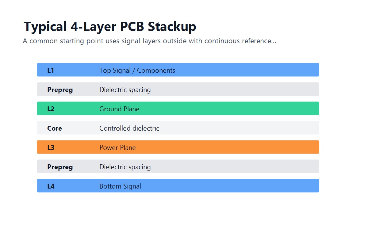
Layer order determines how close signals are to reference planes and how well power and ground planes support the circuit. For example, a common four-layer board may place signal layers on the outside and continuous ground and power planes inside. This can provide a better return path than a simple two-layer board and can also help reduce noise.
However, there is no universal best stackup. A low-speed control board, high-current power board, RF module, high-speed digital board, and compact wearable device may all need different priorities. The correct stackup depends on routing density, signal speed, current level, thermal needs, component packages, board thickness, and manufacturing capability.
Good stackup planning
Critical signals have nearby reference planes, copper is balanced, power paths are clear, and the fabricator can confirm material and thickness assumptions.
Risky stackup planning
Signals cross plane splits, impedance assumptions are unclear, dielectric thickness is guessed, and fabrication questions appear after files are released.
Reference Planes and Return Paths
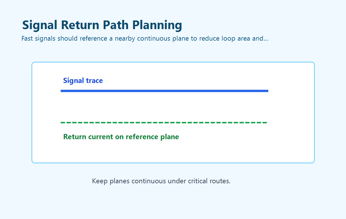
Every signal current has a return current. At higher frequencies, the return current tends to flow close to the signal trace on the nearest reference plane. If that plane is continuous, the loop area stays smaller and the signal path is easier to control. If the trace crosses a split plane, void, or poorly connected reference area, the return path may detour and create noise or EMI risk.
This is why stackup planning and routing rules should be discussed together. Assigning a signal layer without assigning its reference plane leaves a gap in the design intent. Critical clocks, differential pairs, high-speed buses, RF traces, and sensitive analog signals should have clear return-path planning before routing begins.
Impedance Control Starts With the Stackup
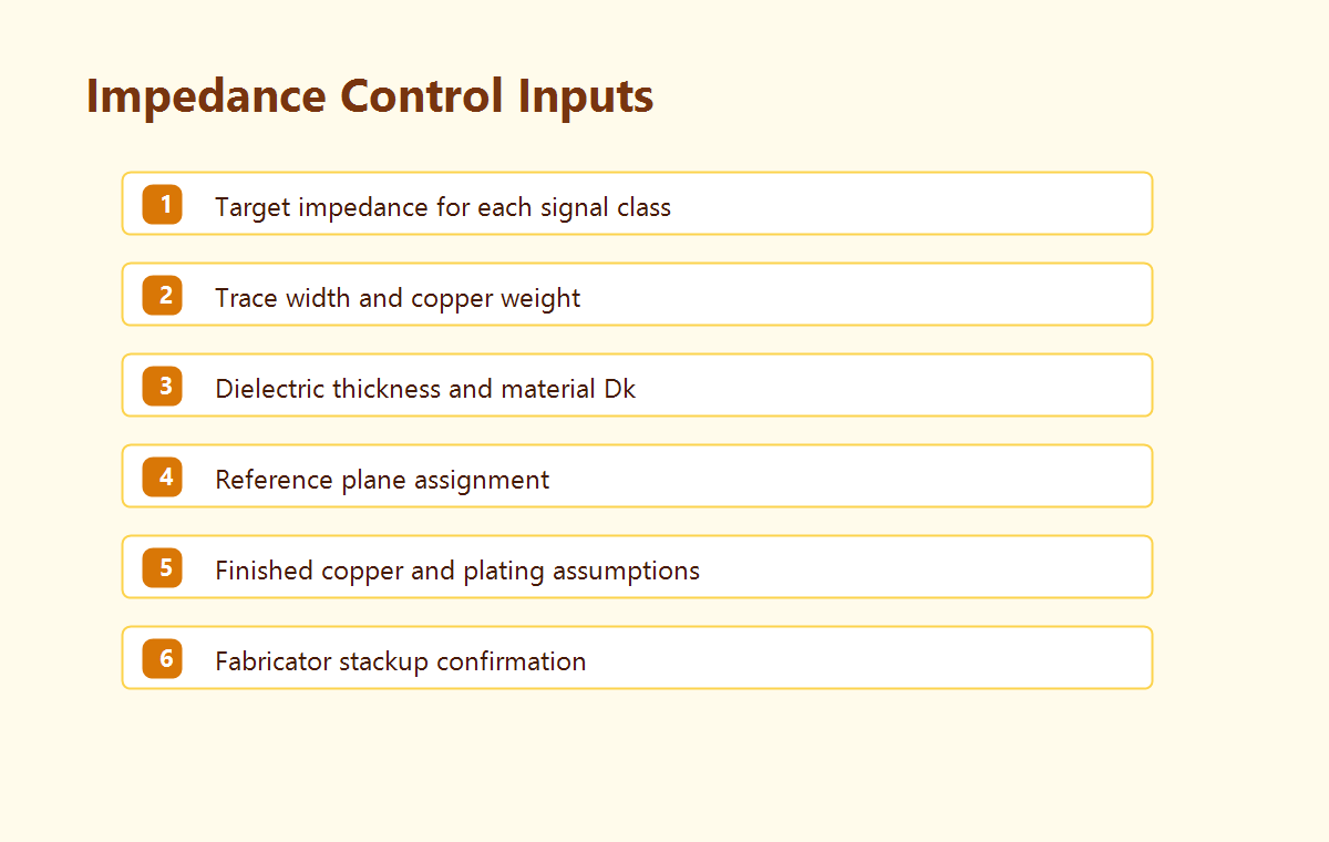
Controlled impedance is not achieved by trace width alone. It depends on trace geometry, copper thickness, dielectric thickness, dielectric constant, solder mask, reference plane distance, and fabrication tolerance. If the stackup is uncertain, impedance targets are also uncertain.
Before ordering a controlled-impedance PCB, the design package should clearly identify which nets need impedance control and what target values apply. Common examples include USB, Ethernet, HDMI, PCIe, LVDS, RF lines, and other high-speed or differential signals. The fabricator may adjust trace width or dielectric spacing to match actual materials and process capability.
Common Stackup Mistakes
- Choosing layer count only by routing convenience without considering return paths.
- Routing fast signals across split planes or gaps in the reference layer.
- Specifying impedance targets without confirming dielectric thickness and material data.
- Using unbalanced copper distribution that can increase warpage risk.
- Leaving power-plane strategy unclear until late in layout.
- Sending manufacturing files without a stackup table or impedance notes.
What to Include in a Stackup Handoff
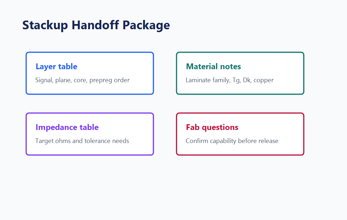
A clean stackup handoff should describe the layer order, copper weights, material assumptions, board thickness, impedance requirements, special reliability needs, and any constraints that the fabricator should confirm. If the design requires specific material families or dielectric values, those details should be stated clearly instead of being left as assumptions.
| Handoff Item | Why It Matters |
|---|---|
| Layer table | Shows signal, plane, core, and prepreg order. |
| Material notes | Clarifies laminate, Tg, dielectric assumptions, and copper requirements. |
| Impedance table | Defines target values for critical single-ended or differential traces. |
| Fabricator confirmation | Helps align design assumptions with real production capability. |
Practical Stackup Review Checklist
- Confirm whether the board needs two, four, six, or more layers based on routing density and signal requirements.
- Assign a continuous reference plane for critical signal layers.
- Keep high-speed signals away from plane splits and poorly stitched return paths.
- Confirm copper weight, board thickness, dielectric thickness, and material assumptions.
- Define controlled-impedance nets before layout release.
- Ask the fabricator to confirm stackup feasibility before production files are finalized.
Conclusion
PCB stackup design connects electrical performance with manufacturability. By planning layer order, reference planes, materials, impedance targets, and handoff notes early, engineering teams can reduce uncertainty and help the board move more smoothly from layout to fabrication and assembly.