
PCB Quality Control Guide
PCB Testing Methods Guide: AOI, X-Ray, ICT, and Functional Testing
PCB testing is not one single step at the end of production. It is a layered quality strategy that combines visual inspection, hidden-joint analysis, electrical verification, and real operating checks so assembly problems can be caught before they become field failures.
As boards become denser, more component packages move under the device body, and customers expect faster delivery, relying on a final visual check is no longer enough. A good PCB test plan answers three practical questions: what defects are most likely, which test method can detect them, and how early in production the issue can be found.
For a manufacturer such as CircFab, where PCB fabrication, SMT assembly, through-hole assembly, inspection, and production support are connected in one workflow, test planning is also a communication tool. It helps engineering, purchasing, assembly, and quality teams work from the same defect-risk map instead of treating testing as a separate afterthought.
Why PCB Testing Needs Multiple Methods
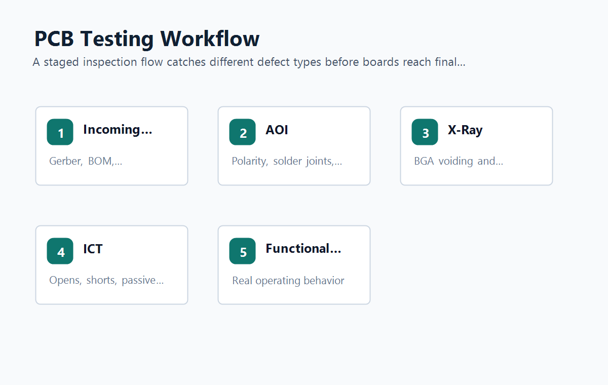
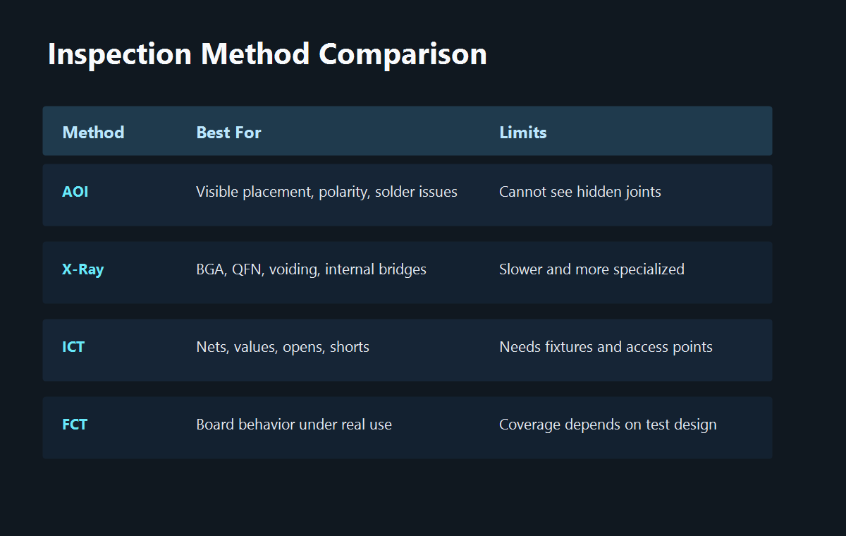
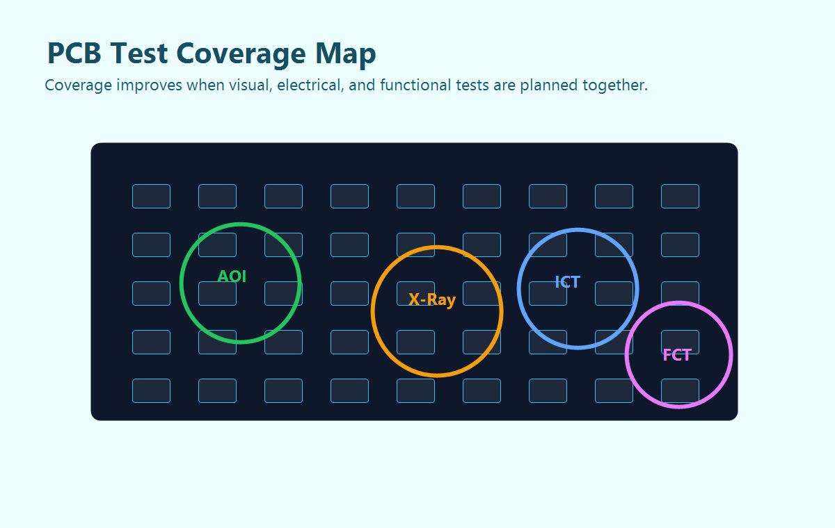
No single PCB inspection method can see every problem. AOI is fast and effective for visible solder and placement defects, but it cannot inspect hidden BGA joints. X-ray can see hidden solder structures, but it is not a functional proof that the circuit behaves correctly. ICT is strong for electrical continuity and component-value checks, but it depends on test access. Functional testing validates real behavior, but it may not identify the exact physical cause of a failure.
Process defects
Missing components, wrong orientation, solder bridges, insufficient solder, tombstoning, and contamination are usually created during assembly and are often caught by AOI, X-ray, or ICT.
Design or documentation defects
Wrong footprints, unclear polarity markings, poor test-point coverage, and incomplete test instructions often require DFM review and production feedback to prevent repeated failures.
1. AOI: Fast Visual Inspection for Assembly Defects
Automated Optical Inspection, or AOI, uses cameras and image-processing software to compare the assembled board against expected placement and solder patterns. It is commonly used after SMT reflow because it can scan boards quickly and flag visible issues before more expensive downstream testing begins.
AOI is especially useful for checking missing parts, skewed components, polarity errors, solder bridges, insufficient solder, and obvious package damage. It works best when component libraries, lighting, and acceptable tolerance windows are tuned for the product rather than copied blindly from a generic template.
2. X-Ray Inspection: Seeing Hidden Solder Joints
X-ray inspection is used when important solder joints are hidden below a package. BGAs, QFNs, LGAs, shielded modules, and some power packages cannot be fully evaluated from the surface. X-ray helps detect voiding, solder bridges under components, insufficient ball collapse, and misalignment that would be invisible to normal optical inspection.
X-ray should be used selectively. It adds cost and time, so it is most valuable for high-risk packages, first-article builds, reliability-sensitive products, and boards where hidden-joint failures would be difficult or expensive to diagnose later.
3. ICT: Electrical Checks Before Final Operation
In-Circuit Testing, often shortened to ICT, checks assembled boards electrically at the node or component level. It can detect opens, shorts, wrong resistor or capacitor values, reversed diodes, and some IC orientation problems. For production programs, ICT can provide fast pass/fail feedback and detailed fault isolation.
The biggest constraint is access. ICT requires test pads, fixture planning, stable board support, and enough spacing for probes. If test access is not considered during PCB layout, the test coverage may be limited. This is why test-point planning should be part of the DFM review before the board is released for manufacturing.
4. Functional Testing: Proving the Board Works
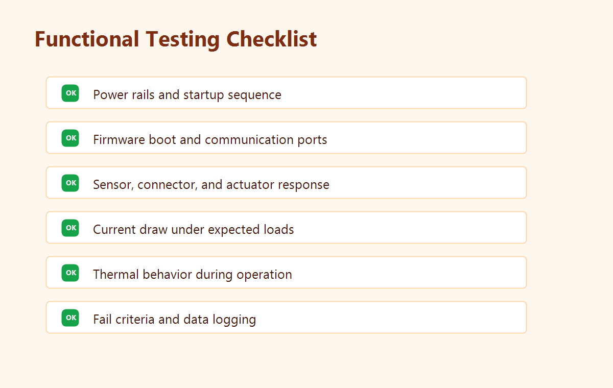
Functional Circuit Testing, or FCT, validates the board under conditions that resemble the final product environment. Instead of only checking whether each component is present or each net is connected, FCT checks whether the assembled circuit performs its intended job.
A functional test may verify power-up sequence, firmware boot, communication ports, LED behavior, sensor response, current draw, relay switching, wireless operation, or connector behavior. The best functional tests are specific, repeatable, and connected to clear pass/fail limits.
How to Choose the Right PCB Test Strategy
The right test strategy depends on board complexity, product risk, production volume, package types, and available test access. A simple prototype may only need DFM review, AOI, and a basic power-on check. A dense production board with BGAs, fine-pitch ICs, and safety-related functions may need AOI, selective X-ray, ICT, programming, and final functional testing.
| Situation | Recommended Test Focus |
|---|---|
| Low-volume prototype | DFM review, AOI, power-on check, manual functional validation |
| BGA or QFN assembly | AOI plus selective X-ray for hidden solder joints |
| Repeat production build | AOI, ICT where access allows, functional test, yield tracking |
| High-reliability product | Layered inspection, documented limits, traceability, corrective-action feedback |
Testing Should Feed Back Into Manufacturing
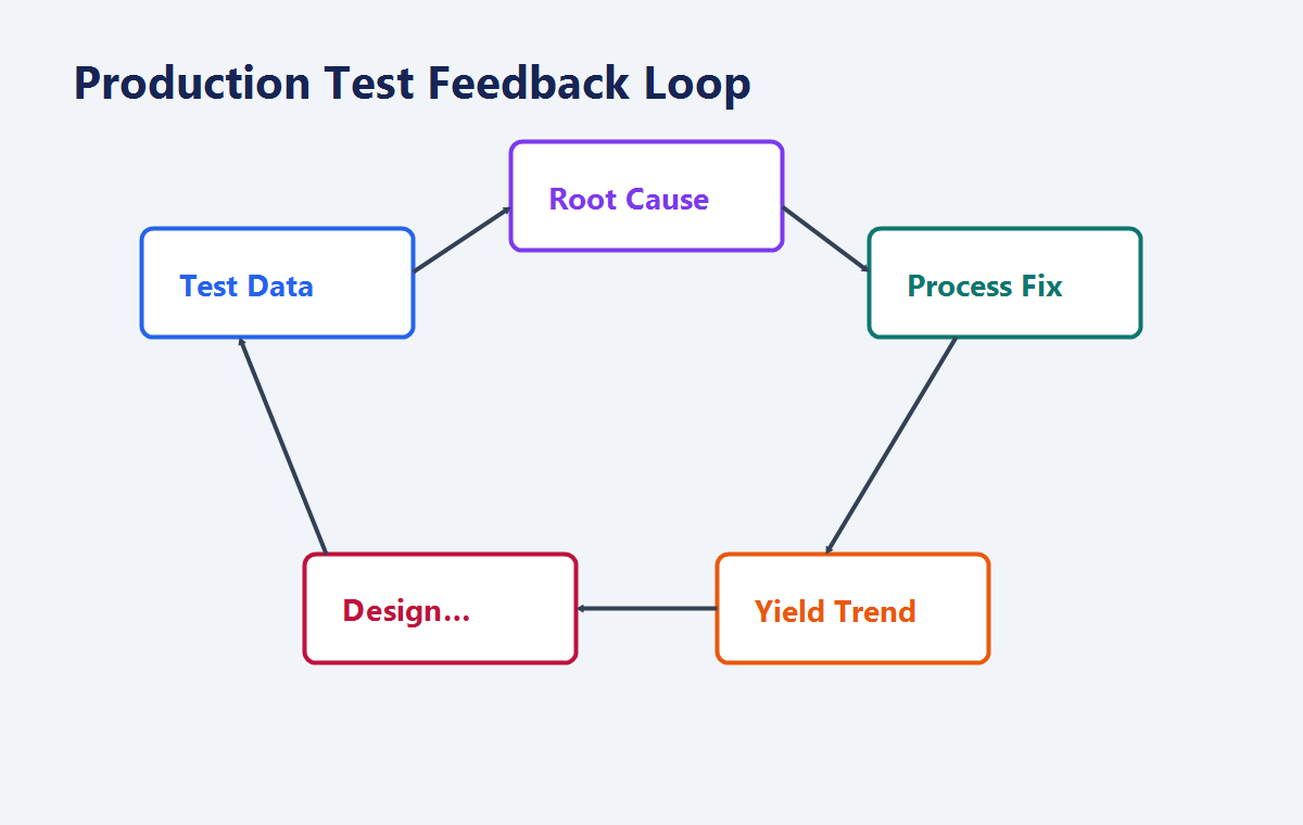
Testing is most valuable when the results improve the next build. If AOI repeatedly finds tombstoning on the same part, the team should review pad design, stencil aperture, placement pressure, and reflow profile. If ICT finds recurring opens on one connector, the fixture, solder process, and component handling should be checked. If functional testing finds intermittent startup failures, engineering may need to review power sequencing, firmware timing, or tolerance stack-up.
Practical Checklist Before You Send a Board for Assembly
- Define which tests are required for prototype, pilot, and production stages.
- Add accessible test points for power rails, communication buses, programming, and key signals.
- Identify BGA, QFN, and bottom-terminated components that may need X-ray inspection.
- Provide firmware, fixtures, cables, test limits, and expected current values before production starts.
- Document acceptable cosmetic, solder, and functional criteria so pass/fail decisions are consistent.
- Review test data after each build and convert repeated failures into process or design improvements.
Conclusion
A strong PCB test plan combines AOI, X-ray, ICT, and functional testing according to the actual risk of the product. The goal is not to add every possible test. The goal is to apply the right method at the right point in production, catch defects early, and use the results to make every following build more reliable.