
What Is a Printed Circuit Board?
A printed circuit board, or PCB, is the foundation of most modern electronic products. It provides both the mechanical support and the electrical pathways that allow components to work together. From consumer electronics and industrial controllers to automotive systems, medical devices, and communication equipment, PCBs make electronic products smaller, more reliable, and easier to manufacture at scale.
A PCB is usually made from an insulating base material, such as FR-4, polyimide, or a specialized laminate. Thin copper layers are patterned into traces, pads, and planes that carry signals and power across the board. Components such as resistors, capacitors, integrated circuits, connectors, sensors, and power devices are mounted onto the board to form a complete electronic circuit.
Common Types of PCBs
Different products require different PCB structures. Rigid PCBs are the most common type and are widely used in consumer electronics, computers, appliances, and industrial equipment. They offer strong mechanical stability and are cost-effective for many standard applications.
Flexible PCBs use bendable materials that allow the circuit to fold or move inside compact assemblies. They are often used in cameras, displays, wearable devices, and products where space is limited. Rigid-flex PCBs combine rigid and flexible sections, helping engineers reduce connectors, save space, and improve durability in complex electronic assemblies.
PCB Stack-Up and Layer Structure
A PCB may have one layer, two layers, or many layers depending on the complexity of the circuit. Multilayer PCBs use alternating copper and dielectric layers to support dense routing, power distribution, ground planes, and controlled signal performance.
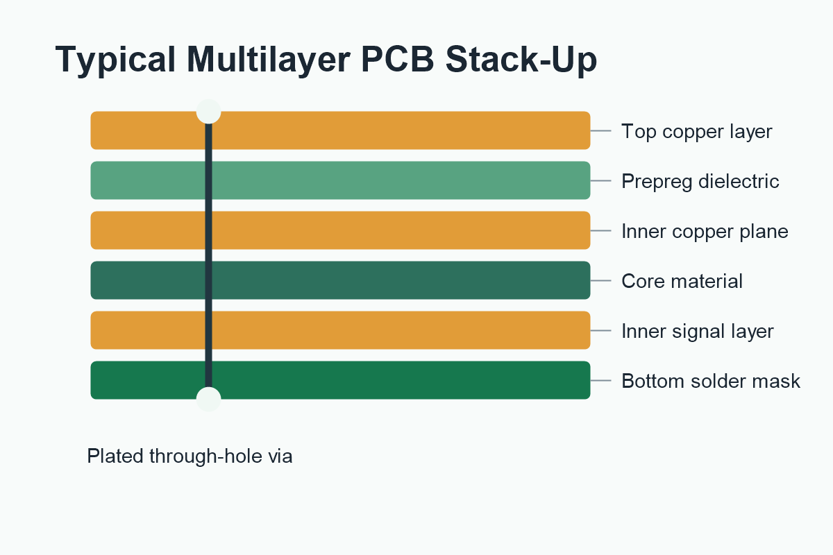
The stack-up is especially important for high-speed, RF, power, and compact electronic products. A well-designed stack-up helps control impedance, reduce electromagnetic interference, improve thermal behavior, and support stable product performance.
PCB Design and Manufacturing Workflow
The PCB development process usually begins with a schematic. Engineers define the circuit, choose components, and determine how signals and power should move through the product. The next stage is PCB layout, where component placement, routing, vias, copper planes, and the board outline are planned.
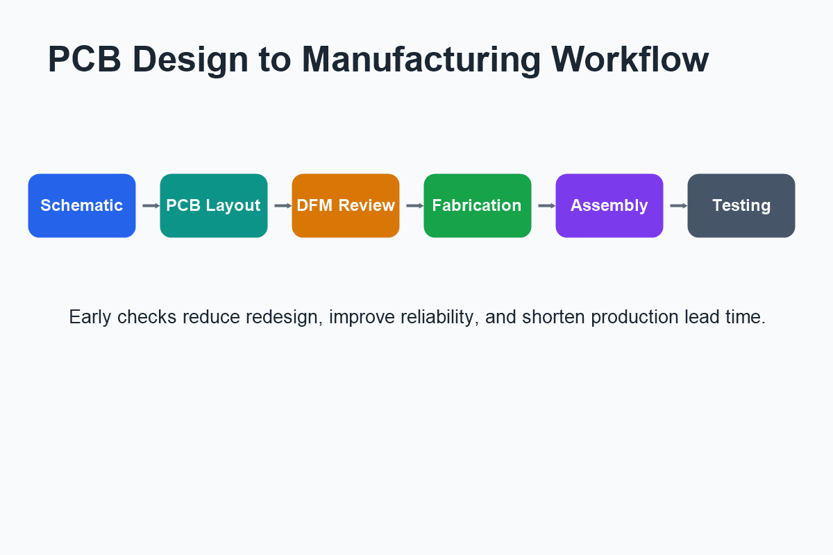
Before fabrication, a design for manufacturability review is important. This step checks whether the board can be produced reliably and efficiently. Issues such as trace spacing, drill sizes, annular rings, copper balance, solder mask clearance, and panelization can affect the final quality and cost of the PCB.
Why Manufacturing Quality Matters
PCB manufacturing includes many steps, including imaging, etching, lamination, drilling, plating, solder mask application, surface finishing, routing, and testing. A small error in any stage can lead to electrical failure, poor soldering, reduced reliability, or production delays.
As electronic products become smaller, faster, and more powerful, PCB requirements continue to increase. Multilayer boards, HDI structures, controlled impedance, thermal management, and flexible materials are now common across many industries. Working with an experienced PCB manufacturing partner helps reduce design risks, improve reliability, and shorten the path from prototype to production.
Conclusion
A printed circuit board is more than a carrier for electronic components. It is a critical part of product performance, manufacturability, and long-term reliability. By understanding PCB structure, design rules, stack-up planning, and manufacturing requirements, engineering teams can build better electronic products with fewer delays and fewer redesigns.